- 您现在的位置:买卖IC网 > Sheet目录336 > IXDS430SI (IXYS)IC DRVR MOSF/IGBT 30A 28-SOIC
�� �
�
�IXDN430� /� IXDI430� /� IXDD430� /� IXDS430�
�OUTPUT LEAD INDUCTANCE�
�Of� equal� importance� to� Supply� Bypassing� and� Grounding� are�
�issues� related� to� the� Output� Lead� Inductance.� Every� effort�
�should� be� made� to� keep� the� leads� between� the� driver� and� it’s�
�load� as� short� and� wide� as� possible.� If� the� driver� must� be� placed�
�farther� than� 2”� from� the� load,� then� the� output� leads� should� be�
�treated� as� transmission� lines.� In� this� case,� a� twisted-pair�
�should� be� considered,� and� the� return� line� of� each� twisted� pair�
�should� be� placed� as� close� as� possible� to� the� ground� pin� of� the�
�driver,� and� connect� directly� to� the� ground� terminal� of� the� load.�
�TTL to High Voltage CMOS Level Translation�
�(IXDD430 Only)�
�The� enable� (EN)� input� to� the� IXDD430� is� a� high� voltage�
�CMOS� logic� level� input� where� the� EN� input� threshold� is� ?�
�V� CC� ,� and� may� not� be� compatible� with� 5V� CMOS� or� TTL� input�
�levels.� The� IXDD430� EN� input� was� intentionally� designed�
�for� enhanced� noise� immunity� with� the� high� voltage� CMOS�
�logic� levels.� In� a� typical� gate� driver� application,� V� CC� =15V�
�and� the� EN� input� threshold� at� 7.5V,� a� 5V� CMOS� logical� high�
�input� applied� to� this� typical� IXDD430� application’s� EN� input�
�A� TTL� or� 5V� CMOS� logic� low,� V� TTLLOW� =~<0.8V,� input� applied� to� the�
�Q1� emitter� will� drive� it� on.� This� causes� the� level� translator�
�output,� the� Q1� collector� output� to� settle� to� V� CESATQ1� +�
�V� TTLLOW� =<~2V,� which� is� sufficiently� low� to� be� correctly� interpreted�
�as� a� high� voltage� CMOS� logic� low� (<1/3V� CC� =5V� for� V� CC� =15V� given�
�in� the� IXDD430� data� sheet.)�
�A� TTL� high,� V� TTLHIGH� =>~2.4V,� or� a� 5V� CMOS� high,�
�V� 5VCMOSHIGH� =~>3.5V,� applied� to� the� EN� input� of� the� circuit� in�
�Figure� 29� will� cause� Q1� to� be� biased� off.� This� results� in� Q1�
�collector� being� pulled� up� by� R3� to� V� CC� =15V,� and� provides� a�
�high� voltage� CMOS� logic� high� output.� The� high� voltage� CMOS�
�logical� EN� output� applied� to� the� IXDD430� EN� input� will� enable�
�it,� allowing� the� gate� driver� to� fully� function� as� an� 30� Amp�
�output� driver.�
�The� total� component� cost� of� the� circuit� in� Figure� 29� is� less�
�than� $0.10� if� purchased� in� quantities� >1K� pieces.� It� is�
�recommended� that� the� physical� placement� of� the� level�
�translator� circuit� be� placed� close� to� the� source� of� the� TTL� or�
�CMOS� logic� circuits� to� maximize� noise� rejection.�
�will� be� misinterpreted� as� a� logical� low,� and� may� cause�
�undesirable� or� unexpected� results.� The� note� below� is� for�
�optional� adaptation� of� TTL� or� 5V� CMOS� levels.�
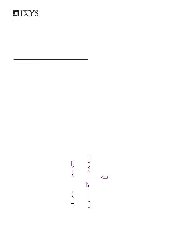
�The� circuit� in� Figure� 29� alleviates� this� potential� logic� level�
�misinterpretation� by� translating� a� TTL� or� 5V� CMOS� logic�
�input� to� high� voltage� CMOS� logic� levels� needed� by� the�
�IXDD430� EN� input.� From� the� figure,� V� CC� is� the� gate� driver�
�power� supply,� typically� set� between� 8V� to� 20V,� and� V� DD� is�
�the� logic� power� supply,� typically� between� 3.3V� to� 5.5V.�
�Resistors� R1� and� R2� form� a� voltage� divider� network� so�
�that� the� Q1� base� is� positioned� at� the� midpoint� of� the�
�expected� TTL� logic� transition� levels.�
�Figure� 29� -� TTL� to� High� Voltage� CMOS� Level� Translator�
�Vcc�
�(From� gate� driver�
�power� supply)�
�(From� logic�
�Vdd�
�power� supply)�
�R3�
�10K�
�R1�
�10K�
�Q1�
�High� Voltage�
�CMOS� EN� output�
�(To� IXDD430� EN� input)�
�2N3904�
�R2�
�10K�
�5V� CMOS� or� TTL� input�
�EN�
�IXYS� Corporation�
�3540� Bassett� St;� Santa� Clara,� CA� 95054�
�Tel:� 408-982-0700;� Fax:� 408-496-0670�
�www.ixys.com�
�e-mail:� sales@ixys.net�
�12�
�IXYS� Semiconductor� GmbH�
�Edisonstrasse15� ;� D-68623;� Lampertheim�
�Tel:� +49-6206-503-0;� Fax:� +49-6206-503627�
�e-mail:� marcom@ixys.de�
�DS99045A(8/03)�
�发布紧急采购,3分钟左右您将得到回复。
相关PDF资料
IXS839S1T/R
IC MOSFET DRIVER SYNC BUCK 8SOIC
JLINK-RX-AD
ADAPT BD FOR MINI-JTAG CONNECTOR
JMBADGE2008-B
BOARD JM BADGE
JP9902
CONN JACK MOD INSERT W/O HOLES
JTAGJET-C2000
JTAG EMULATOR FOR TI C2000 MCU
JTAGJET-CCS
JTAG EMULATOR TI C2000/5000/6000
JTAGJET-OMAP3
JTAG EMULATOR OMAP3 W/DEBUGGER
JTAGJET-TRACE-4M
JTAG EMULATOR W/4M TRACE BUFFER
相关代理商/技术参数
IXDS502D1B
功能描述:功率驱动器IC 2 Amps V 4 Rds RoHS:否 制造商:Micrel 产品:MOSFET Gate Drivers 类型:Low Cost High or Low Side MOSFET Driver 上升时间: 下降时间: 电源电压-最大:30 V 电源电压-最小:2.75 V 电源电流: 最大功率耗散: 最大工作温度:+ 85 C 安装风格:SMD/SMT 封装 / 箱体:SOIC-8 封装:Tube
IXDT30N120
功能描述:IGBT 晶体管 60 Amps 1200V 2.4 Rds RoHS:否 制造商:Fairchild Semiconductor 配置: 集电极—发射极最大电压 VCEO:650 V 集电极—射极饱和电压:2.3 V 栅极/发射极最大电压:20 V 在25 C的连续集电极电流:150 A 栅极—射极漏泄电流:400 nA 功率耗散:187 W 最大工作温度: 封装 / 箱体:TO-247 封装:Tube
IXDT30N120AU1
制造商:未知厂家 制造商全称:未知厂家 功能描述:TRANSISTOR | IGBT | N-CHAN | 1.2KV V(BR)CES | 50A I(C) | TO-268AA
IXDT30N120D1
制造商:IXYS 制造商全称:IXYS Corporation 功能描述:High Voltage IGBT with optional Diode
IXE5216EC.C0
制造商:Intel 功能描述:Electronic Component
IXE611P1
功能描述:IC DRIVER MOSF/IGBT HALF 8-PDIP RoHS:是 类别:集成电路 (IC) >> PMIC - MOSFET,电桥驱动器 - 外部开关 系列:- 标准包装:50 系列:- 配置:高端 输入类型:非反相 延迟时间:200ns 电流 - 峰:250mA 配置数:1 输出数:1 高端电压 - 最大(自引导启动):600V 电源电压:12 V ~ 20 V 工作温度:-40°C ~ 125°C 安装类型:通孔 封装/外壳:8-DIP(0.300",7.62mm) 供应商设备封装:8-DIP 包装:管件 其它名称:*IR2127
IXE611S1
功能描述:IC DRIVER MOSF/IGBT HALF 8-SOIC RoHS:是 类别:集成电路 (IC) >> PMIC - MOSFET,电桥驱动器 - 外部开关 系列:- 标准包装:50 系列:- 配置:高端 输入类型:非反相 延迟时间:200ns 电流 - 峰:250mA 配置数:1 输出数:1 高端电压 - 最大(自引导启动):600V 电源电压:12 V ~ 20 V 工作温度:-40°C ~ 125°C 安装类型:通孔 封装/外壳:8-DIP(0.300",7.62mm) 供应商设备封装:8-DIP 包装:管件 其它名称:*IR2127
IXE611S1T/R
功能描述:功率驱动器IC 0.6 Amps 35V 25 Rds RoHS:否 制造商:Micrel 产品:MOSFET Gate Drivers 类型:Low Cost High or Low Side MOSFET Driver 上升时间: 下降时间: 电源电压-最大:30 V 电源电压-最小:2.75 V 电源电流: 最大功率耗散: 最大工作温度:+ 85 C 安装风格:SMD/SMT 封装 / 箱体:SOIC-8 封装:Tube